Bit-Slice Design: Controllers and ALUs
by Donnamaie E. White
Copyright © 1996, 2001, 2002 Donnamaie E. White
- Pre-Introduction
- Selection of the Implementation
- Microprogramming
- Advantages of LSI
- The 2900 Family
- Language Interrelationships
- Controller Design
- Constructing the CCU
- Sequential Execution
- Multiple Sequences
- Start Addresses
- Mapping PROM
- Unconditional Branch
- Conditional Branch
- Timing Considerations
- Pipelining
- Improved Architecture
3. Adding Programming
Support to the Controller
- Expanded Testing
- Subroutines
- Nested Subroutines
- Stack Size
- Loops
- Am29811
- Am2909/11
- CASE Statement (Am29803A)
- Microprogram Memory
- Status Polling
- Interrupt Servicing
- Implementation - Interrupt Request Signals
- Vector Mapping PROM
- Next Address Control
- Am2910
- Am2910 Instructions
- Control Lines
- Interrupt Handling
- Am2914
- Interconnection of the Am2914
6. The ALU and Basic Arithmetic
- Further Enhancements
- Instruction Fields
- Instruction Set Extensions
- Sample Operations
- Arithmetic -- General
- Multiplication with the Am2901
- Am2903 Multiply
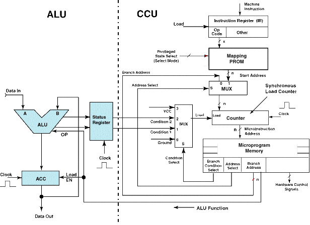
Simple Controller continuedLast Edit April 3, 1997; May 1, 1999; July 9, 2001 Timing ConsiderationsThe basic controller evolved so far can be a primitive CCU. Figure 2-16 shows the connections between this CCU and the ALU portions of the simple system described earlier. Figure 2-16 Elementary System
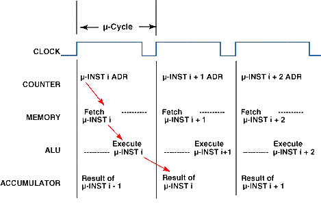
The clock pulse width, called the microcycle, is determined from the maximum propagation delay from clock to output plus the maximum time delay for PROM read access plus the maximum time for ALU execution. (For the 2900 family, a microcycle is measured from one rising edge of the clock to the next. Rather traditional. All register write operations occur on the rising edge of the clock.) CP = tcounter clock to output + tPROM read accree + tALU execution All times are maximum worst-case. Sequential TimingA timing diagram is given in Figure 2-17 showing a series of sequential program steps (refer to the CCU-ALU of Figure 2-16). At each rising edge of the clock, the counter increments and settlers, and the counter oputputs an address of the PROM, whose access time is greater than the counter settling time. As soon as the outputs are stable at the PROM output, execution begins in the ALU. (For now, assume that the operands are available.) On the next rising edge of the clock, the ALU result is gated into the accumulator and the status signals which are being input into the condition MUX are sassumed to be stable. (They would normally be gated into a status register on the same clock edge that loads the accumulator.) Figure 2-17 Microcycle Timing for the System of Figure 2-16 (no branch)
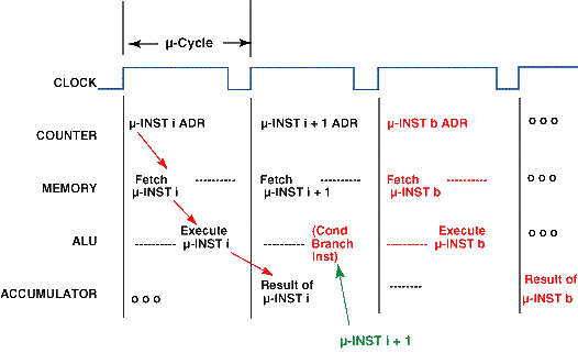
BranchingNow assume that a conditional branch is to be executed. On the rising edge of the clock, the status signals from the previous instruction and the result of that instruction are available. Concurrently, the counter has been incremented (Figure 2-18). (Note this counter is a synchronous loading counter.) The microinstruction i+ 1 has been fetched, and this is the conditional branch. Figure 2-18 Microcycle Timing for the System of Figure 2-16 (branch). Conditional branch on result of previous microinstruction.
When the outputs are available from the PROM memory, the control signals are sent to the counter to cause it to load the branch address if the tested condition is TRUE. The MUX select bits, and the condition inputs propagate directly through the MUX prior to the next rising edge of the clock. No ALU activity occurs. On the next rising edge of the clock, the branch address enters the counter and the address is input to the PROM. Execution proceeds as before. There is no difference in the instruction cycle of a branch address and a nonbranch instruction in this system. However, while the memory is being accessed, the ALU must remain idle, and while the ALU executes, the memory must remain idle. The minimum total width of the microcycle, CP, is the sum of the worst-case fetch and execute times. |