Bit-Slice Design: Controllers and ALUs
by Donnamaie E. White
Copyright © 1996, 2001, 2002 Donnamaie E. White
- Pre-Introduction
- Selection of the Implementation
- Microprogramming
- Advantages of LSI
- The 2900 Family
- Language Interrelationships
- Controller Design
- Constructing the CCU
- Sequential Execution
- Multiple Sequences
- Start Addresses
- Mapping PROM
- Unconditional Branch
- Conditional Branch
- Timing Considerations
- Pipelining
- Improved Architecture
3. Adding Programming
Support to the Controller
- Expanded Testing
- Subroutines
- Nested Subroutines
- Stack Size
- Loops
- Am29811
- Am2909/11
- CASE Statement (Am29803A)
- Microprogram Memory
- Status Polling
- Interrupt Servicing
- Implementation - Interrupt Request Signals
- Vector Mapping PROM
- Next Address Control
- Am2910
- Am2910 Instructions
- Control Lines
- Interrupt Handling
- Am2914
- Interconnection of the Am2914
6. The ALU and Basic Arithmetic
- Further Enhancements
- Instruction Fields
- Instruction Set Extensions
- Sample Operations
- Arithmetic -- General
- Multiplication with the Am2901
- Am2903 Multiply
Evolution of the ALU
Last Edit July 11, 2001
The basic controller is well-defined at this point in the design. If
a CCU is being developed, the next step is the development of an appropriate
ALU and the other related modules which will comprise the CPU of the system
as well as the interconnect to the main read-write system memory.
Instruction Formats
The simple ALU shown in Figure 5-1 has
- an ALU, with carry-in and function control coming from the CCU
- an ACC register, with load enable control coming from the CCU.
Figure 5-1a Simple System
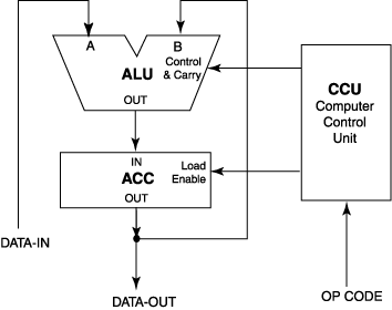
This simple system could support ADD, SUB, OR, EXOR, LOAD ACC, or PASS. The assumption was made that data same in only on the A port of the ALU and therefore that the instruction had the form:
Figure 5-1b Single Address Instruction
|
Op Code |
Operand
Address
|
This is only one of many forms that could occur among various systems or within one system.
There are often several formats for instructions in a system, of which some of the more typical for direct addressing are:
- op-code with implied operand
- op-code with single address
- op-code with two addresses
- op-code with three addresses
Literals, indexed registers, indirect addresses, base-relative addresses, register addresses, and combinations of these are ignored here.
Control Unit Function
As a computer control, the CCU must be able to direct the fetch of the op-code to the instruction register and decode whether or not part of the instruction contains an address. If it does, that address must be gated into the MAR, which will then be used to fetch the actual data from memory. In the simple system being described, the op code will be gated into the IR (instruction register) at the same time that the address is gated into the MAR.
If a memory fetch for data is required, the decode of the op code will produce the required microinstructions to perform the actual fetch. Once all of the operands are available, the ALU function execution proceeds. In the simple system being described, the fetch of the second operand occurs in the same microcycle as the ALU execute.
PC and MAR
Involved in the above memory fetch operations are two registers, the PC and the MAR. The PC (program counter) stores the address of the next machine-level (macro) instruction to be fetched from the program area of the main memory. The MAR (memory address register) contains the address which is to be placed on the main memory address bus. The address will be either that transferred from the PC register (instruction fetch) or that loaded from an instruction (data fetch). In the SIMCOM (simple computer) system, only the MAR connects to the address bus, although both the PC and MAR could be used to supply an address to the memory, at the cost of increased complexity in the bus structure. Both the PC and the MAR are loaded from the ALU output as shown in Figure 5-2.
Figure 5-2 Expanded System

Now assume that the program is executing an arithmetic ADD and that address i is in the PC register. This is the address of the next instruction to be fetched (see Figure 5-3).
Figure 5-3 Single address operation of SIMCOM. The PC contains the address of the instruction to be fetched. It transfers its contents to the MAR and then increments. The MAR is used to address memory. The instruction (in this example) is brought out to the instruction register (IR) and to the memory address register (MAR). The IR contains the op code to be decoded by the CCU. The MAR contains the address of the operand which must be fetched before the op code is executed.

The PC register contents are placed on the main memory address bus via the MAR, and the contents at address i are fetched and loaded into the instruction register (IR) and the MAR.
The MAR register contents (address j) are placed on the memory address bus under the control of the CCU and the contents of the storage location at address j are fetched and input to the data input port of the ALU.
At the same time, the ACC passes its contents to the other part of the ALU and the CCU sends a control instruction to the ALU. These three events are coordinated so that the two operands arrive at the same instant I ± tc ( tc is some allowable error, some unit of time). The ALU is ready to process them when they arrive. On the next clock, the result is loaded into the ACC. The PC is incremented and execution continues.
The design in Figure 5-2 uses the ALU to increment the PC register and could place the result either in the PC register or in both the PC and MAR registers. The MAR cannot input to the PC register in this configuration.
Also shown is a connection to the ACC outputs such that the test for <ACC> = 0 is possible. There are no other status outputs for the ALU as yet. The test input is connected to the CCU, which is at the moment considered to be an undefined black box.
With this design, the SIMCOM supports a basic instruction set that includes basic arithmetic and logical operations as well as some memory access and branch instructions, as summarized in Table 5-1. INA and OUT allow data to come into or be placed out of the system., via the data bus, to an unspecified location. The arithmetic and logical operations and the LDA and STO operations assume that the op address format is processed as described earlier. The JMP and JMZ instructions assume that the PC is loaded with the address provided within the instruction.
Table 5-1 Basic Instruction Set
| LDA, Addr | Load accumulator with contents of address (main memory) |
| ADD, Addr | Add accumulator and contents of address |
| SUB, Addr | Subtract accumulator from contents of address |
| OR, Addr | OR accumulator and contents of address |
| AND, Addr | AND accumulator and contents of address |
| XOR, Addr | Exclusive-OR accumulator and contents of address |
| INA | Input to accumulator (from data bus) |
| OUT | Output from accumulator (to data bus) |
| JMP, Addr | Jump to address (GO TO) |
| JMZ, Addr | Jump to address IF accumulator is 0, <ACC> = 0 |
| STO, Addr | Store contents of accumulator at address (main memory) |