Bit-Slice Design: Controllers and ALUs
by Donnamaie E. White
Copyright © 1996, 2001, 2002 Donnamaie E. White
- Pre-Introduction
- Selection of the Implementation
- Microprogramming
- Advantages of LSI
- The 2900 Family
- Language Interrelationships
- Controller Design
- Constructing the CCU
- Sequential Execution
- Multiple Sequences
- Start Addresses
- Mapping PROM
- Unconditional Branch
- Conditional Branch
- Timing Considerations
- Pipelining
- Improved Architecture
3. Adding Programming
Support to the Controller
- Expanded Testing
- Subroutines
- Nested Subroutines
- Stack Size
- Loops
- Am29811
- Am2909/11
- CASE Statement (Am29803A)
- Microprogram Memory
- Status Polling
- Interrupt Servicing
- Implementation - Interrupt Request Signals
- Vector Mapping PROM
- Next Address Control
- Am2910
- Am2910 Instructions
- Control Lines
- Interrupt Handling
- Am2914
- Interconnection of the Am2914
6. The ALU and Basic Arithmetic
- Further Enhancements
- Instruction Fields
- Instruction Set Extensions
- Sample Operations
- Arithmetic -- General
- Multiplication with the Am2901
- Am2903 Multiply
The ALU and Basic ArithmeticLast Edit November 1, 1996; May 1, 1999 ; July 15, 2001 Sample OperationsSome operations will be examined fro the two-RALU slices, the Am2901 ans the Am2903. [AMD also did an Am29203 that was released after this book was published.] IncrementIt is desired to increment a register and at the same time output its original value:
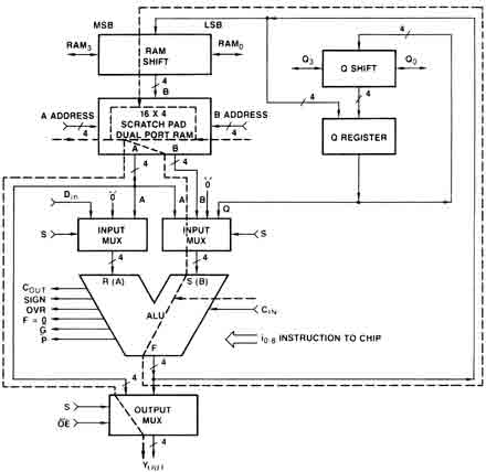
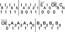
Assume that the register is B15 and that it has been previously loaded with a value. If it has not been previously loaded with a value, the contents are unknown and undetermined. Am2901 Version The Am2901 microcontrols are derived by examining each subfield table. The A and B addresses will both be F16. The only way to output from a scratchpad is to select A with the output MUX. This leaves the B,0 pair as the source control.; therefore I2I1I0 is set at 38. The ALU function is add or increment; therefore I5I4I3 is set to 08, and CN is set to 18. The result of the ADD is to be passed around from the ALU output F to the RAM shift register and then to the scratchpad memory, to R15. This is the destination control F--> B, A --> Y; therefore I8I7I6 is set to 288. The complete microword for the Am2901 is: The data flow is given in Figure 6-3. Figure 6-3 Am2901: Increment a register and output its original value
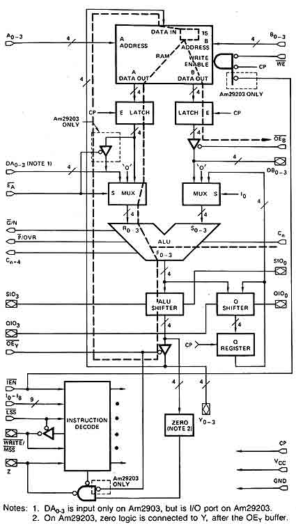
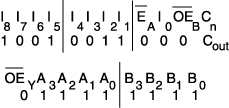
Am2903 Version The same problem approach is used with the Am2903. The only way to output directly from the scratchpad is via the DBout path, which requires OE'n be held LOW. The ALU will add A + 0; therefore I4I3I2I1 will be set to 616, Cin set to 1, and I0 set to 0. The A port input MUX select E'A is set LOW. The A and B addresses are set to F16, assuming that R15 is in use. Since Y will be used to input back into the scratchpad, OEY = LOW and WE' will be driven by WRITE'/MSS'. The complete microword for the Am2903 is: The data flow is given in Figure 6-4. Figure 6-4 Am2903: Increment a register and output its original value
Byte SwapA 16-bit byte swap exchanges bits B15-B8, with B7-B0 in order and visa versa. Assume a 16-bit ALU (4 slices) and that the register is question is R15. Am2901 Version The Am2901 microcode solution can be constructed by taking advantage of the fact that a shift up is equivalent to multiplying by 2. If the result of an add of R15 + R15 is shifted (prior to storing the result) into R15, the effect is a 2-bit rotate, assuming that
Since we are selecting source operands as A, B, adding, and shifting, 2F --> B; the microword is: The microinstruction must be repeated four times to cause an 8-bit rotate, for a total timing of four microcycles of approximately 165 ns worst-case minimum (dependent onthe actual hardware). [Remember that this was the late 1970s and early 1980s - times change.] Am2903 Version The Am2903 solution is approached in the same way. The S shift is connected for rotate as was the RAM shift of the Am2901. The carry out is input to the carry in, and an ADD is performed. The complete microword is: Am2901 Hardware Version The byte-swap operation can be performed faster using additional hardware (such as Am25LS240/244) tristate buffers (select noninverting). The Am2901 Y outputs are gated out to the budders, which in turn input to the appropriate DA inputs of another Am2901. The operation performed by the Am2901 in this case is to output from the scratchpad, Y -> A, and to pass the DA input through the ALU and back into the scratchpad memory, F -> B. The additional hardware allows the byte swap to be done in one microcycle. The microword is: Am2903 Hardware Version There are two ways to perform a hardware-assisted byte swap using the Am2903 and the Am25LS240/244 buffers. One approach is to use the DB as the output to the buffers and to use DA as the input point. This is the relatively slower approach, since the DA input passes the data through the ALU and back to the scratchpad. The other approach uses the Y port as the data input, which provides a datapath directly into the scratchpad. This method avoids the propagation delay of the ALU, shift register, tristate buffer, and input MUX. The microwords are: The basic difference is the OEY control.
|


