| |
Chapter 4
Coverage Analysis in the Design Flow
Current ASIC Design flow
The modern ASIC design flow has evolved and increased in complexity just as the devices that are being designed have dramatically increased in complexity. This design flow is now heavily dependent on EDA tools and many of the tasks that were once carried out manually are now automated by EDA tools with little or no manual intervention.
As a function of this increase in complexity it has been necessary for designers and verification engineers to seek out higher levels of abstraction to carry out their respective tasks.
This abstraction of the design process means that designers develop their designs in hardware description languages such as Verilog and VHDL. These languages not only allow designers to describe logic gates; they can also specify abstract types, such as the states of a state machine, and complex operations, such as multiply, in a single line of HDL code.
So powerful are these hardware description languages that two levels of abstraction in the design flow are now possible; namely, RTL (Register Transfer Level) and Behavioral level.
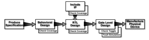
The design flow including these two levels of abstraction is shown in Figure 4-1.
As with all design projects the flow starts with a specification. Currently there is no universally accepted way of capturing a specification. Usually it is a complex written document that immediately runs the risk of containing ambiguities. It is for this reason that many large design companies employ two teams - a design team and verification team both working from the same specification. The idea here is that any ambiguities are trapped using this two-pronged attack.
From the specification a behavioral description of the design is generated. Currently this process has to be done manually. Normally the behavioral description is captured in a hardware description language such as VHDL or Verilog or even C++. Once the behavioral description has been captured the designer has a formal unambiguous circuit description that can be executed and therefore tested against the specification. This is an important stage in the process because already at this early stage the design can be tested for misconceptions. Bringing in verification as early as possible is critical in the modern design process because the process is so long sometimes months or even years and discovering a major conceptual error late in the design process would result in significant time and cost over-runs. Whether using VHDL or Verilog - or a combination of both languages, verification is usually carried out using one of the many commercially available HDL simulators.
The design is tested by applying a number of stimuli, test vectors or test benches - usually written in the same language as the design - and checking the resulting responses. This may be done either manually or automatically if the simulator allows it and if the expected responses are included in what is then known as a self-checking test bench.
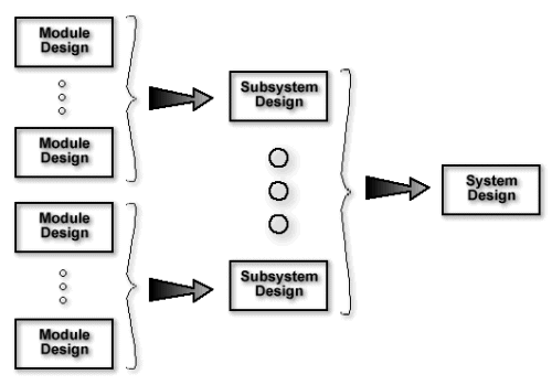
Having verified the behavioral design the next step in the process is to decompose this to an RTL description. While RTL is still a level of abstraction above gate level, the design blocks, combinational logic and registers can be clearly identified. In fact 80% of a design's structure is typically fixed at the RTL stage. Transforming a design from a behavioral description into RTL is still a largely manual process. Most of the functional verification (in terms of time spent) is done at the RTL stage. HDL simulation is the most frequently used functional verification technique - most designers and verification engineers having access to at least one simulator. The RTL design process is potentially the most significant task in the design process and is therefore usually further subdivided as shown in Figure 4-2.
The first step is to divide the functionality into a number of blocks, modules or design units. Once these modules have been developed and tested they are merged into subsystems and then the functionality of these items is verified. Finally the subsystems are integrated into the full system and it is verified. By subdividing the problem more development engineers can work in parallel to reduce the overall project time.
After completing the RTL design the next step is to transform this description into a gate level description in the target ASIC technology. This process is known as logic synthesis and is now predominantly a fully automatic process, with more than one software package available in the market today. Again the functionality of the system is verified at gate level although this process usually involves using timing data from automatic place and route tools to make the simulations as accurate as possible. The purpose of the verification at this stage is to determine that the system operates correctly with the timing constraints of the physical ASIC device. Gate level simulations take significantly longer than RTL simulations.
The other operation that is performed on the gate level description is Fault Simulation. The purpose of this is to create a set of tests which will be used to verify the actual ASIC is free from production defects once it has been manufactured. These tests can bare little relationship to the functionality of the device. Fault simulations take much greater simulation effort than normal functional simulations.
The final stage in the process, once the physical layout has been completed, is to manufacture the actual devices, after which the tests created by fault simulation can be run to verify the manufacturing process.
Coverage Analysis in the Design Flow
Coverage analysis identifies the parts of your HDL code that are executed during simulation and, more importantly, highlights the parts of the code that have not been executed. You may think that it is obvious to a designer what has been tested, but this is very often not the case. The problem is made far worse when there are separate design and verification teams working on the same project. Figure 4-3 shows the problem graphically. Initially the amount of HDL code tested increases rapidly but, as the verification process continues, the rate at which HDL code is covered decreases until finally it is very difficult to determine whether all the HDL code has been executed.
This uncertainty of what has been executed is a big risk to the project. Any code that has not been tested may contain errors and the effect of these errors is completely unknown. Should one of these errors be found later in the project, for example during gate level simulation, or after the device has been manufactured the cost of fixing the problem is much greater - as indicated in Figure 4-4. Not only is the cost a problem, but the project time-scales could be seriously compromised and the company could miss the window of opportunity for the product.

Figure 4-5 shows the effect of applying coverage analysis to the project. Each simulation that is run with coverage analysis shows the areas of the design that have not yet been tested so that the next batch of tests can target the untested functionality. This coverage directed verification process gives the design and verification team much greater confidence that their design has been 100% tested. In addition coverage directed verification means that less time is wasted re-testing parts of the design that have already been covered and more time is spent on targeting the untested areas of the design.
Coverage analysis not only helps with the verification process. It also helps with planning and time-scale estimation. Coverage analysis gives continuous feedback on what proportion of the design is left to be verified and, based on the time taken so far, an accurate estimate of how much time is required to complete the testing.
There are number of coverage analysis tools for Verilog available today. One of the most comprehensive and well established of these is Verification Navigator from TransEDA. Verification Navigator is also the only true VHDL coverage analysis tool on the market.
There are three occasions during the design flow described earlier where the functionality of the design is verified. These are at the behavioral level, at the RTL level and at the gate level. However, because 80% of the design structure is set at the RTL stage, and RTL design is carried out using either VHDL or Verilog, it is the RTL level that is the most suitable stage for using coverage analysis.
RTL design comprises three basic parts 1) module design, 2) subsystem integration 3) system integration as shown in Figure 4-6. Verification is carried out at all three of these stages and therefore it is appropriate to use coverage analysis at each of these stages. By ensuring that a module is thoroughly verified before it is integrated into the rest of the design, the risk of finding a problem later in the design cycle is significantly reduced. It is also much easier to test individual blocks than a complete system.
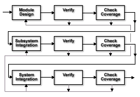
Coverage analysis is still applicable once the modules have been integrated together to form subsystems and systems to ensure that the glue logic that joins the modules is fully tested and that all possible operations of the module have been tested within the bounds of the system.
Coverage analysis does not need to be used only at the RTL stage; behavioral design is also often done using VHDL and Verilog and it is just as important to ensure the behavioral level design is fully executed. Fully testing the behavioral design ensures that all the design concepts have been fully explored.
Gate level descriptions can be expressed as Verilog or VHDL netlists. These netlists, however, do not contain any of the constructs that are usually tested with coverage analysis. In fact the only things that can be examined at gate level are the signals in the design. This does not mean that coverage analysis is a waste of time at gate level because Verification Navigator and a few of the other coverage analysis tools can perform a check known as Toggle Coverage. Toggle coverage is useful as a measure of the amount of data applied to gate level descriptions and as a pre-cursor to fault simulation.
Figure 4-7 shows the design flow described above.
IP in the Design Flow
Modern designs have become so large that a single device can be a whole system on a chip (SoC). It is for this reason that many chip design teams now use IP (intellectual property). These are cores of functionality which have been already written in a HDL and can be easily included in a design. IP cores can be devices that were once large ICs; for example - the Pentium processor. The idea behind using IP blocks is to save on design effort. In actual fact the cost of using an IP block is between 30% and 100% of the time to design the block from scratch depending on the quality of the IP core. IP blocks are always written in RTL so that they can be synthesized. Figure 4-8 shows the design flow including IP blocks.
When employing an IP block it is essential to know the quality of the test benches that accompany that block. It is for this reason that coverage analysis should be used on the IP block, just as it would be used on a block developed as part of the project.
In addition, it is essential to continue to apply coverage analysis to the IP block when it has been integrated into the design, in order to verify that the interface to the IP block has been fully tested and that all aspects of the block's behavior have been tested within the bounds of your system. Figure 4-9 shows the process of IP integration including verification with coverage analysis.
Today's ASIC design flow is a long and complex process because of the size and sophistication of the devices being produced. It is for this reason that it is critical that the devices are `right first time'. If they are not, a failure in the field is not only costly but it is technologically embarrassing and is likely to also be financially detrimental. In addition, the window of opportunity can be missed and market share lost - sometimes irrecoverably. It pays to ensure that the products that are released will meet the customers' expectations - which means that extensive verification must be carried out. Major semiconductor manufacturers now realise this and that is why, in many companies, design verification can account for up to 70% of the total cost of the entire design process.
Because of the relative cost, any tool that makes this verification process more reliable and shorter has to be a `must have'. The feedback that coverage analysis produces is invaluable in making the verification process more reliable, timescales more predictable and generally aiding the whole process.
|
|
|