17.3.1
Clock Routing
Gate arrays normally use a clock spine (a regular grid), eliminating the need for special routing (see Section 16.1.6, “Clock Planning”). The clock distribution grid is designed at the same time as the gate-array base to ensure a minimum clock skew and minimum clock latency—given power dissipation and clock buffer area limitations. Cell-based ASICs may use either a clock spine, a clock tree, or a hybrid approach.
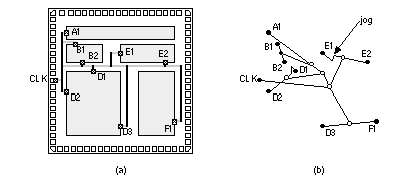
Figure 17.21
shows how a clock router may minimize clock skew in a clock spine by making the path lengths, and thus net delays, to every leaf node equal—using jogs in the interconnect paths if necessary. More sophisticated clock routers perform
clock-tree synthesis
(automatically choosing the depth and structure of the clock tree) and
clock-buffer insertion
(equalizing the delay to the leaf nodes by balancing interconnect delays and buffer delays).
|

|
|
FIGURE 17.21
Clock routing. (a) A clock network for the cell-based ASIC from Figure 16.11. (b) Equalizing the interconnect segments between CLK and all destinations (by including jogs if necessary) minimizes clock skew.
|
The clock tree may contain multiply-driven nodes (more than one active element driving a net). The net delay models that we have used break down in this case and we may have to extract the clock network and perform circuit simulation, followed by back-annotation of the clock delays to the netlist (for circuit extraction, see
Section 17.4
) and the bus currents to the clock router. The sizes of the clock buses depend on the current they must carry. The limits are set by reliability issues to be discussed next.
Clock skew induced by hot-electron wearout was mentioned in Section 16.1.6, “Clock Planning.” Another factor contributing to unpredictable clock skew is changes in clock-buffer delays with variations in power-supply voltage due to data-dependent activity. This
activity-induced clock skew
can easily be larger than the skew achievable using a clock router. For example, there is little point in using software capable of reducing clock skew to less than 100 ps if, due to fluctuations in power-supply voltage when part of the chip becomes active, the clock-network delays change by 200 ps.
The power buses supplying the buffers driving the clock spine carry direct current (
unidirectional current or DC), but the clock spine itself carries alternating current (
bidirectional current or AC). The difference between
electromigration
failure rates due to AC and DC leads to different rules for sizing clock buses. As we explained in Section 16.1.6, “Clock Planning,” the fastest way to drive a large load in CMOS is to taper successive stages by approximately
e
ª
3. This is not necessarily the smallest-area or lowest-power approach, however [
Veendrick, 1984].
17.3.2
Power Routing
Each of the power buses has to be
sized
according to the current it will carry. Too much current in a power bus can lead to a failure through a mechanism known as
electromigration
[Young and Christou, 1994]. The required power-bus widths can be estimated automatically from library information, from a separate
power simulation
tool, or by entering the
power-bus widths to the routing software by hand. Many routers use a default power-bus width so that it is quite easy to complete routing of an ASIC without even knowing about this problem.
For a
direct current (
DC) the
mean time to failure
(
MTTF) due to electromigration is experimentally found to obey the following equation:
|
MTTF
|
=
|
A
J
–2
exp
–
E
/
k
T
,
|
|
(17.9)
|
where
J
is the current density;
E
is approximately 0.5 eV;
k
, Boltzmann’s constant, is 8.62
¥
10
–5
eVK
–1
; and
T
is absolute temperature in kelvins.
There are a number of different approaches to model the effect of an AC component. A typical expression is
|
|
|
A
J
–2
exp
–
E
/
k
T
|
|
|
|
MTTF
|
=
|
–––––––––––––––––––––––––
|
,
|
(17.10)
|
|
|
|
J
|
J
|
+ k
AC/DC
|
J
|
2
|
|
|
where
J
is the average of
J(t)
, and
|
J
|
is the average of | J |. The constant
k
AC/DC
relates the relative effects of AC and DC and is typically between 0.01 and 0.0001. Electromigration problems become serious with a MTTF of less than 10
5
hours (approximately 10 years) for current densities (DC) greater than 0.5 GAm
–2
at temperatures above 150 °C.
Table 17.1
lists example
metallization reliability rules
—limits for the current you can pass through a metal layer, contact, or via—for the typical 0.5
m
m three-level metal CMOS process,
G5. The limit of 1 mA of current per square micron of metal cross section is a good rule-of-thumb to follow for current density in aluminum-based interconnect.
Some CMOS processes also have
maximum metal-width rules
(or
fat-metal rules
). This is because
stress (especially at the corners of the die, which occurs during
die attach
—mounting the die on the chip carrier) can cause large metal areas to lift. A solution to this problem is to place slots in the wide metal lines. These rules are dependent on the ASIC vendor’s level of experience.
To determine the power-bus widths we need to determine the bus currents. The largest problem is emulating the system’s operating conditions. Input vectors to test the system are not necessarily representative of actual system operation. Clock-bus sizing depends strongly on the parameter
k
AC/DC
in Eq.
17.10
, since the clock spine carries alternating current. (For the sources of power dissipation in CMOS, see Section 15.5, “Power Dissipation.”)
Gate arrays normally use a regular
power grid
as part of the gate-array base. The gate-array logic cells contain two fixed-width power buses inside the cell, running horizontally on m1. The horizontal m1 power buses are then strapped in a vertical direction by m2 buses, which run vertically across the chip. The resistance of the power grid is extracted and simulated with SPICE during the base-array design to model the effects of IR drops under worst-case conditions.
|
TABLE 17.1
Metallization reliability rules for a typical 0.5 micron ( l = 0.25
m
m) CMOS process.
|
|
Layer/contact/via
|
Current limit
|
Metal thickness
|
Resistance
|
|
m1
|
1 mA
m
m
–1
|
7000 Å
|
95 m
W
/square
|
|
m2
|
1 mA
m
m
–1
|
7000 Å
|
95 m
W
/square
|
|
m3
|
2 mA
m
m
–1
|
12,000 Å
|
48 m
W
/square
|
|
0.8
m
m square m1 contact to diffusion
|
0.7 mA
|
|
11
W
|
|
0.8
m
m square m1 contact to poly
|
0.7 mA
|
|
16
W
|
|
0.8
m
m square m1/m2 via (via1)
|
0.7 mA
|
|
3.6
W
|
|
0.8
m
m square m2/m3 via (via2)
|
0.7 mA
|
|
3.6
W
|
Standard cells are constructed in a similar fashion to gate-array cells, with power buses running horizontally in m1 at the top and bottom of each cell. A row of standard cells uses
end-cap cells
that connect to the VDD and VSS power buses placed by the power router. Power routing of cell-based ASICs may include the option to include vertical m2 straps at a specified intervals. Alternatively the number of standard cells that can be placed in a row may be limited during placement. The power router forms an interdigitated comb structure, minimizing the number of times a VDD or VSS power bus needs to change layers. This is achieved by routing with a
routing bias
on preferred layers. For example, VDD may be routed with a left-and-down bias on m1, with VSS routed using right-and-up bias on m2.
Three-level metal processes either use a m3 with a thickness and pitch that is comparable to m1 and m2 (which usually have approximately the same thickness and pitch) or they use metal that is much thicker (up to twice as thick as m1 and m2) with a coarser pitch (up to twice as wide as m1 and m2). The factor that determines the m3/4/5 properties is normally the sophistication of the fabrication process.
In a three-level metal process, power routing is similar to two-level metal ASICs. Power buses inside the logic cells are still normally run on m1. Using HVH routing it would be possible to run the power buses on m3 and drop vias all the way down to m1 when power is required in the cells. The problem with this approach is that it creates pillars of blockage across all three layers.
Using three or more layers of metal for routing, it is possible to eliminate some of the channels completely. In these cases we complete all the routing in m2 and m3 on top of the logic cells using connectors placed in the center of the cells on m1. If we can eliminate the channels between cell rows, we can flip rows about a horizontal axis and abut adjacent rows together (a technique known as
flip and abut
). If the power buses are at the top (VDD) and bottom (VSS) of the cells in m1 we can abut or overlap the power buses (joining VDD to VDD and VSS to VSS in alternate rows).
Power distribution schemes are also a function of process and packaging technology. Recall that flip-chip technology allows pads to be placed anywhere on a chip (see Section 16.1.5, “I/O and Power Planning,” especially Figure 16.13d). Four-level metal and aggressive stacked-via rules allow I/O pad circuits to be placed in the core. The problems with this approach include placing the ESD and latch-up protection circuits required in the I/O pads (normally kept widely separated from core logic) adjacent to the logic cells in the core.
