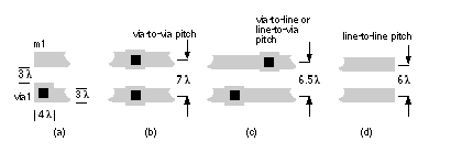
FIGURE 17.9 The metal routing pitch. (a) An example of l -based metal design rules for m1 and via1 (m1/m2 via). (b) Via-to-via pitch for adjacent vias. (c) Via-to-line (or line-to-via) pitch for nonadjacent vias. (d) Line-to-line pitch with no vias.
[ Chapter start ] [ Previous page ] [ Next page ]
The global routing step determines the channels to be used for each interconnect. Using this information the detailed router decides the exact location and layers for each interconnect. Figure 17.9 (a) shows typical metal rules. These rules determine the m1 routing pitch ( track pitch , track spacing , or just pitch ). We can set the m1 pitch to one of three values:
The same choices apply to the m2 and other metal layers if they are present. Via-to-via spacing allows the router to place vias adjacent to each other. Via-to-line spacing is hard to use in practice because it restricts the router to nonadjacent vias. Using line-to-line spacing prevents the router from placing a via at all without using jogs and is rarely used. Via-to-via spacing is the easiest for a router to use and the most common. Using either via-to-line or via-to-via spacing means that the routing pitch is larger than the minimum metal pitch.
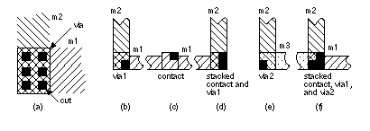
Sometimes people draw a distinction between a cut and a via when they talk about large connections such as shown in Figure 17.10 (a). We split or stitch a large via into identically sized cuts (sometimes called a waffle via ). Because of the profile of the metal in a contact and the way current flows into a contact, often the total resistance of several small cuts is less than that of one large cut. Using identically sized cuts also means the processing conditions during contact etching, which may vary with the area and perimeter of a contact, are the same for every cut on the chip.
In a stacked via the contact cuts all overlap in a layout plot and it is impossible to tell just how many vias on which layers are present. Figure 17.10 (b–f) show an alternative way to draw contacts and vias. Though this is not a standard, using the diagonal box convention makes it possible to recognize stacked vias and contacts on a layout (in any orientation). I shall use these conventions when it is necessary.
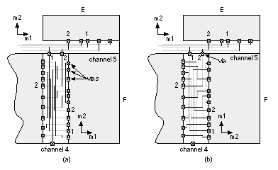
In a two-level metal CMOS ASIC technology we complete the wiring using the two different metal layers for the horizontal and vertical directions, one layer for each direction. This is Manhattan routing , because the results look similar to the rectangular north–south and east–west layout of streets in New York City. Thus, for example, if terminals are on the m2 layer, then we route the horizontal branches in a channel using m2 and the vertical trunks using m1. Figure 17.11 shows that, although we may choose a preferred direction for each metal layer (for example, m1 for horizontal routing and m2 for vertical routing), this may lead to problems in cases that have both horizontal and vertical channels. In these cases we define a preferred metal layer in the direction of the channel spine. In Figure 17.11 , because the logic cell connectors are on m2, any vertical channel has to use vias at every logic cell location. By changing the orientation of the metal directions in vertical channels, we can avoid this, and instead we only need to place vias at the intersection of horizontal and vertical channels.